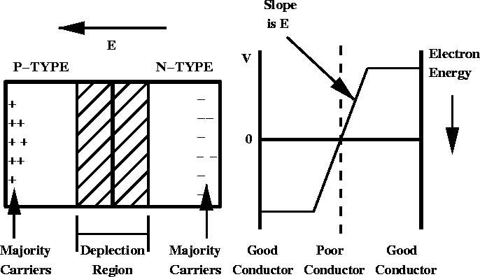
Figure 4.1: PN junction diode.
By joining a P-type and N-type semiconductor together we can make a diode (figure 4.1)

Figure 4.1: PN junction diode.
Initially both semiconductors are totally neutral. The concentration of positive and negative carriers are quite different on opposite sides of the junction and the thermal energy-powered diffusion of positive carriers into the N-type material and negative carriers into the P-type material occurs. The N-type material acquires an excess of positive charge near the junction and the P-type material acquires an excess of negative charge. Eventually diffuse charges build up and an electric field is created which drives the minority charges and eventually equilibrium is reached. A region develops at the junction called the depletion region. This region is essentially un-doped or just intrinsic silicon.
To complete the diode conductor, leads are placed at the ends of the PN junction.
Narippawaj Ngernvijit