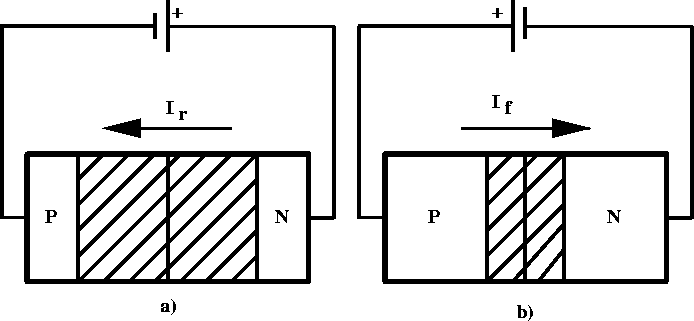
Figure 4.2: Diode circuit connections: a) reversed biased and b) forward biased.
The behaviour of a diode depends on its polarity in the circuit (figure 4.2). If the diode is reverse biased (positive potential on N-type material) the depletion region increases. The only charge carriers able to support a net current across the PN junction are the minority carriers and hence the reverse current is very small. A forward-biased diode (positive potential on P-type material) has a decreased depletion region; the majority carriers can diffuse across the junction. The voltage may become high enough to eliminate the depletion region entirely.
Figure 4.2: Diode circuit connections: a) reversed biased
and b) forward biased.
An approximation to the current in the PN junction region is given by (shown in figure 4.3a)
![]()
where both ![]() and
and ![]() are temperature dependent.
This equation gives a reasonably accurate prediction of the
current-voltage relationship of the PN junction itself - especially
the temperature variation - and can be improved somewhat by choosing
are temperature dependent.
This equation gives a reasonably accurate prediction of the
current-voltage relationship of the PN junction itself - especially
the temperature variation - and can be improved somewhat by choosing
![]() and
and ![]() empirically to fit a particular diode.
However, for a real diode, other factors are also important: in
particular, edge effects around the border of the junction cause the
actual reverse current to increase slightly with reverse voltage, and
the finite conductivity of the doped semi-conductor ultimately
restricts the forward current to a linear increase with increasing
applied voltage.
A better current-voltage curve for the real diode is shown in the
figure 4.3b.
empirically to fit a particular diode.
However, for a real diode, other factors are also important: in
particular, edge effects around the border of the junction cause the
actual reverse current to increase slightly with reverse voltage, and
the finite conductivity of the doped semi-conductor ultimately
restricts the forward current to a linear increase with increasing
applied voltage.
A better current-voltage curve for the real diode is shown in the
figure 4.3b.
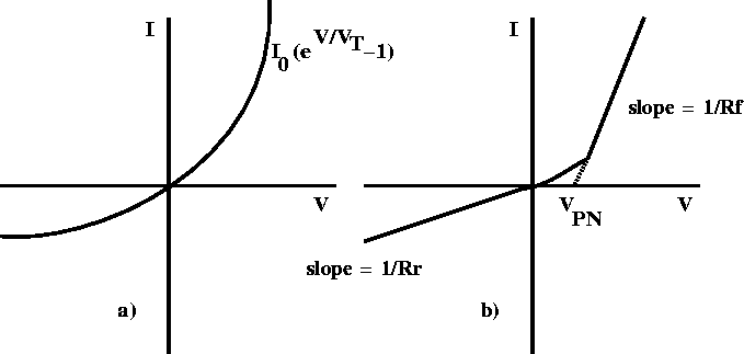
Figure 4.3: Current versus voltage a) in the PN junction
region and b) for an actual PN diode.
Various regions of the curve can be identified: the linear region of
forward-biasing, a non-linear transition region, a turn-on voltage
( ![]() ) and a reverse-biased region.
We can assign a dynamic resistance to the diode in each of the linear
regions:
) and a reverse-biased region.
We can assign a dynamic resistance to the diode in each of the linear
regions: ![]() in the forward-biased region and
in the forward-biased region and ![]() in the
reverse-biased region.
These resistances are defined as the inverse slope of the curve:
in the
reverse-biased region.
These resistances are defined as the inverse slope of the curve:
![]() .
The voltage
.
The voltage ![]() , represents the effective voltage drop across a
forward-biased PN junction (the turn-on voltage).
For a germanium diode,
, represents the effective voltage drop across a
forward-biased PN junction (the turn-on voltage).
For a germanium diode, ![]() is approximately 0.3 V, while for a
silicon diode it is close to 0.6 V.
is approximately 0.3 V, while for a
silicon diode it is close to 0.6 V.